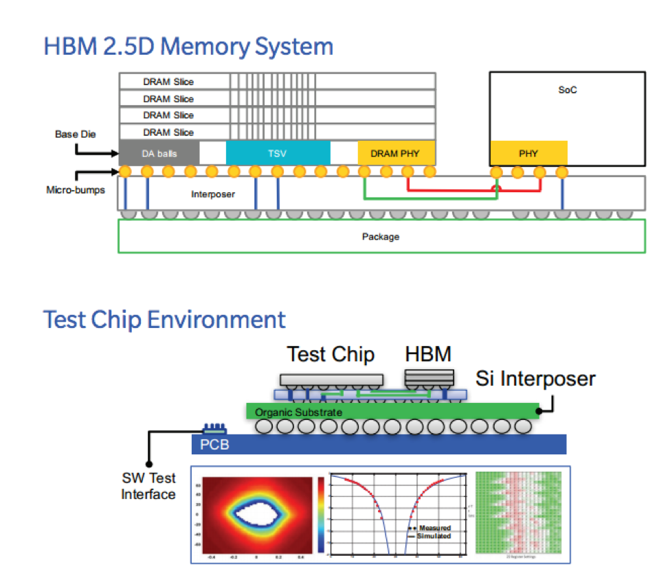
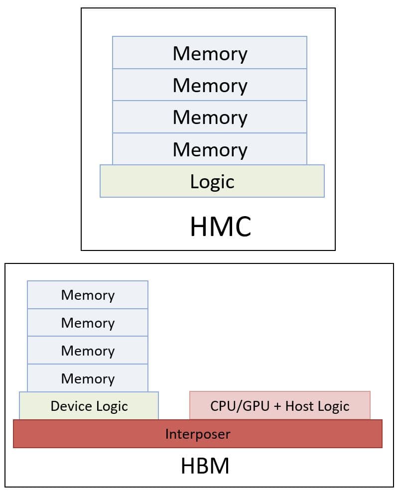
a) General structure of an HBM-enabled device. (b) HBM interface
Par un écrivain mystérieux
Last updated 07 juin 2024
IJMS, Free Full-Text
The Rambus HBM GEN2 PHY: A closer look - Rambus

High Bandwidth Memory (HBM) Architecture - AMD Plans for the Future of GPUs - PC Perspective

Scaling Bump Pitches In Advanced Packaging
The history and future of DRAM architectures in different application domains – an analysis

High-bandwidth memory (HBM) options for demanding applications.
TAPRE-HBM: Trace-Based Processor Rapid Emulation Using HBM on FPGAs
High Bandwidth Memory (HBM) Architecture - AMD Plans for the Future of GPUs - PC Perspective

ThunderGP: Resource-Efficient Graph Processing Framework on FPGAs with HLS
Recommandé pour vous
 HBM PHY Cadence14 Jul 2023
 Revolution of High Bandwidth Memory (HBM) in the Age of AI14 Jul 2023
 HBM Express Official Website14 Jul 2023
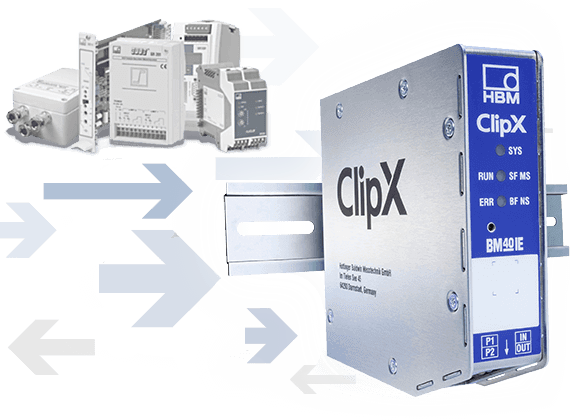 Retrofit Your Automation Systems with ClipX!14 Jul 2023
 NVIDIA Confirmed To Be Supplied With Second Gen. HBM From Both14 Jul 2023
![Eng Sub] HBM Memory Module: Samsung, SK Hynix](https://i.ytimg.com/vi/KyKwiziPmD4/maxresdefault.jpg) Eng Sub] HBM Memory Module: Samsung, SK Hynix14 Jul 2023
Eng Sub] HBM Memory Module: Samsung, SK Hynix14 Jul 2023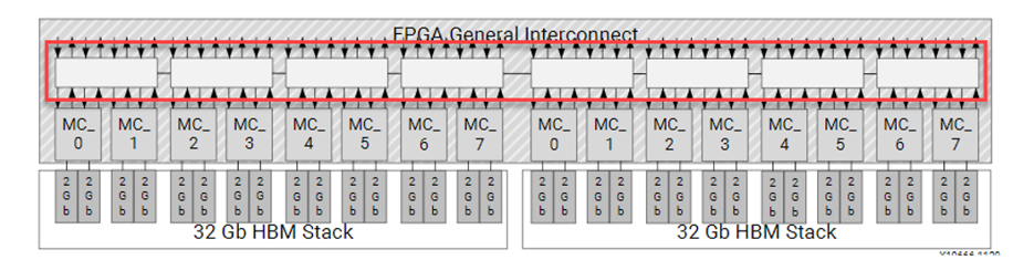 HBM Overview — Vitis™ Tutorials 2021.1 documentation14 Jul 2023
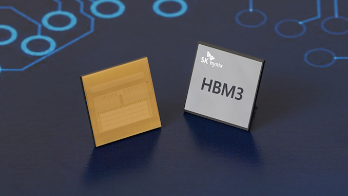 As The Demand for HBM Explodes, SK Hynix is Expected to Benefit14 Jul 2023
 Will HBM replace DDR and become Computer Memory? - Utmel14 Jul 2023
 Renovation of affordable housing (HBM) - Towards a “sustainable14 Jul 2023
Tu pourrais aussi aimer
 WHISKY IRLANDAIS BLACK BUSH 40% BUSHMILLS14 Jul 2023
 Photo Albums in Photo Albums & Refills14 Jul 2023
 Collant de contention Maternité opaque classe 2 par Sigvaris14 Jul 2023
 MKISHINE® Respirant Oreiller Coussin Lombaire Dos Chaise Bureau14 Jul 2023
 Support pour écran intéractif14 Jul 2023
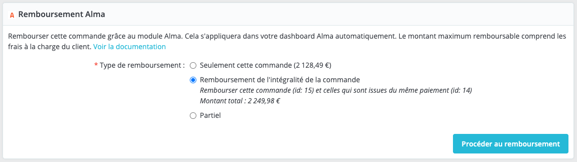 Remboursements via PrestaShop14 Jul 2023
 Gilet réfléchissant Enfant - Universprint14 Jul 2023
 Ponceuse Mirka DEROS 5650CV 125/150mm électrique en coffret14 Jul 2023
 Chaussons Fille pointure 35 - DistriCenter14 Jul 2023
 8 Pièces Joint Carrelage Stylo Joint Carrelage,Joint Carrelage Blanc Stylo,Kit Reparation Carrelage, Stylo de Peinture pour Carrelage de Salle de Bain(Blanche) : : Bricolage14 Jul 2023